
Myths About Using a Via in Pad
The use of via in pad can help PCB designers increase component density and reduce the total trace length on a circuit board. However, there are several important issues associated with using this design technique that should be considered. This guide will examine three major myths surrounding via in pad and offer practical insight into navigating the complexities of this advanced technology.
Using via in pad increases PCB manufacturing costs because it requires additional steps to properly fabricate the board. This includes the use of specialized drilling equipment to accurately create small-diameter via holes and the application of advanced plating techniques to ensure reliable conductive paths within the vias. These additional steps also lead to higher assembly and inspection costs.
In addition, the via caps that are used to prevent air entrapment and outgassing during assembly can add another layer of complexity to the production process. These caps must be properly designed to prevent solder wicking and voids, which can impact the integrity of the electrical connection between the pad and the IC. Additionally, the cap must be a material that can be soldered to without breaking down or becoming brittle during the soldering process.
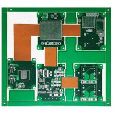
Three Myths About Using a Via in Pad
This additional layer of complexity in the manufacturing process can also cause a delay in the fab cycle. For example, the pcb manufacturer may need to wait longer than usual for the vias to be capped and plated, which can make it more difficult to meet deadlines. As a result, this design technique can be a significant source of cost and delay for your project.
When used correctly, via in pad can provide a number of advantages to the Printed Circuit Board (PCB) layout. For example, it can save space by allowing designers to place bypass capacitors close to their components, which can reduce parasitic inductance and improve signal integrity. Additionally, it can reduce the number of connecting segments for high-speed signals, which can help to reduce signal reflection and noise.
When using a via in pad, it is important to ensure that the shape of the solder stencil openings on the PCB match the shape of the vias. Otherwise, the solder will be deposited on top of the via instead of on the pad. This can cause the circuit to fail because the solder will not form a complete and robust connection to the pad.
One of the primary benefits of using via in pad is the ability to save valuable board space. As devices shrink in size and functionality grows more complex, designers face increasing challenges in routing dense circuits. Traditional vias occupy additional space, requiring a gap between the pad and the via itself. In contrast, via in pad eliminates this need by integrating the via within the pad, optimizing the available area. This technique is particularly beneficial for small form factor devices such as smartphones, wearables, and other portable electronics where every millimeter counts.
While there are some instances where it is necessary to use a via in pad, it should be avoided if possible. This is especially true for small pads, like those on small BGAs or fine pitch components, as it can lead to solder wicking and coplanarity issues. In these cases, it is often better to simply use a smaller via drill, via filling or capping.